This week we learned about pcbs and PCB design and be able to design one ourselves.
Requirements
- Use the test equipment in your lab to observe the operation of a microcontroller circuit board (as a minimum, you should demonstrate the use of a multimeter and oscilloscope)
- Document your work on the group work page and reflect what you learned on your individual page
Group Assignment
Individual Assignment
- Use an EDA tool to design a development board that uses parts from the inventory to interact and communicate with an embedded microcontroller
Softwares 💻
- KiCAD
Group Assignment
In this week we're digging deeper with electronics, what're the most famous one and how to combine them together on a copper traces to create a "Printed Circuit Board" PCB. . and how we measure their properties and what test tools we use that're available in our lab. The most common tools are the Avometer and the Oscilloscope.
Avometer
The Multimeter is a multipurpose tool that can be used to measure the current-unit is Ampere which is the flow of electrons through a circuit Voltage-unit is Volts which is the potential between two points in the circuit Resistance-Unit is Ohms which is the resistance of the circuit Cintinuity of a track or a wire between two points in the circuit.

We uploaded a simple blinking code to arduino nano and measured the voltage change.
Oscilloscope
We went ahead to discover oscilloscope. It's a device that can plots the electrical signal as it varies over time. it plots them as a two-dimensional graph with time on the x-axis and voltage on the y-axis. You have a probe to hook to your circuit and a gnd
The Interface maybe daunting but it comes down to this: A series of knobs with the term vertical and Horizontal. The vertical knobs are used to adjust the voltage, scale it up or down. It has two duttons called "CH1" & "CH2" which refer to the pin your probe is connected To the scope has two channels that can be used. While the horizontal knobs are used to adjust the time scale and position on the graph. The Auto Set button is used to automatically adjust the signal to fit the screen.
Like the previous test on the avometer we went ahead and saw the fading signal on the oscilloscope.
We also how the graph moves in a PWM signal.
logic Analyzer
Once finished with the scope, we learned about logic analyzer. It's a device that can capture signals from the perpherial'spins and make you see the hidden message in the signal like the increption of it and help you decode it in the software.It's as simple as connecting the pins to the analyzer and the analyzer to the computer and you're good to go.
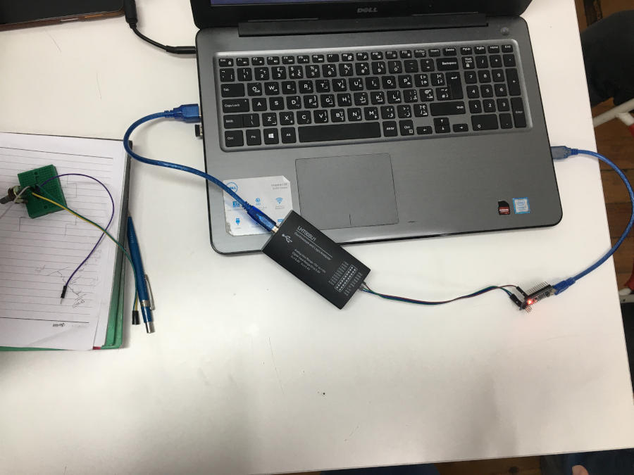
We Then hooked a poentimeter and analyzed's data. we made the capture rate to be 1million sample in 1 second.
After that we analyzed a serial code that said.. did you catch it?
Hello World.
PCBs 101 & How to Build One
Printed Circuit boards are everywhere. if you liked to smash your tv remote control you'll find a green board. Welcome this is the pcb. It's a circuit that combines electrical components in a neat compact place. It's made out of boards which have layers of conductive material "copper" and non-conductive material. The copper is etched using different manufacturing methods usually with Acid to create the traces that connect the components together. But since we're making a prototype we'll use a different method called "Milling" it uses an endmill to carve in the copper and create the connections.
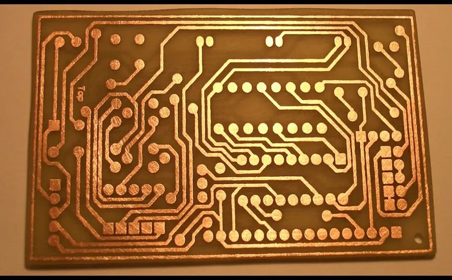
Credits: Viasion Technology
The electronic components mounted on the pcb can passive like resistors, capacitors, etc or active like Integrated circuits. they all can be connected to the pcb using two ways either a through-hole technology (THT) or Surface-mount devices(SMD). We use SMD components because they're smaller and don't require holes to be drilled in the pcb. In this week I learned about the different sizes and packages of SMD Components For example, the most famous packages for resistors and capacitors are the 0603, 1206. The number refers to the size of the component in millimeters. And Whenever you're stuck with a component you can refer to the digikey library. This is very important since each package has a different footprint and to make sure you have the correct component in your pcb, you can always check this site . Also this site is very helpful to read the SMD Resistor Codes.
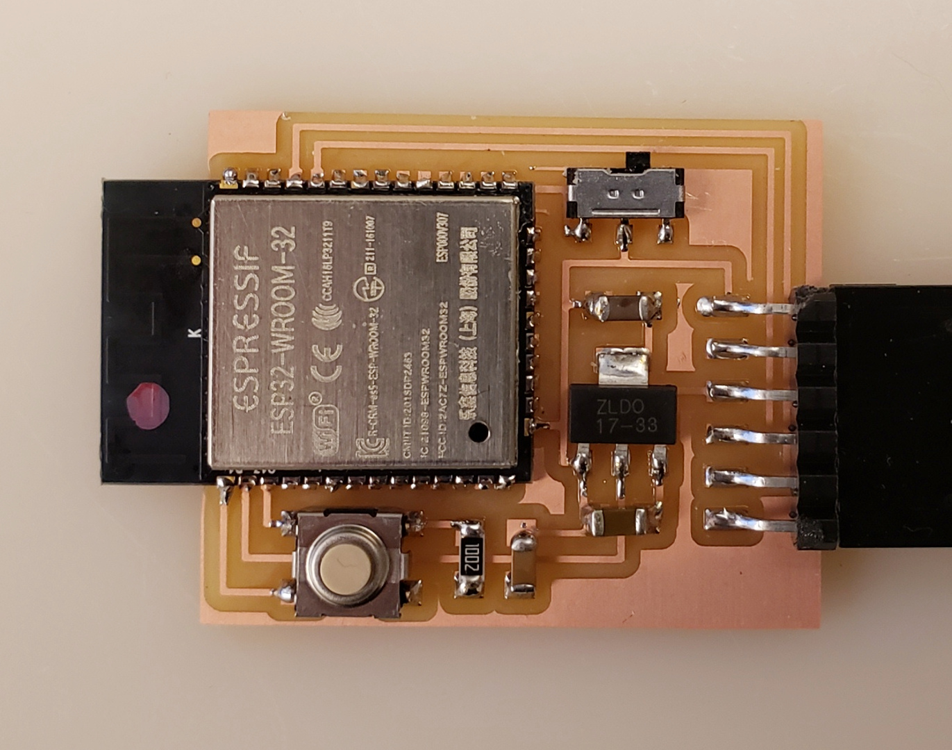
My PCB
Let's start with my simple pcb. I want to build a pcb with ESP32-Wroom module that has a led as output and a switch as input to meet the requirements for this week. And has some pinheaders for I2C and 1 pin for PWM to use it in the input and output devices weeks.It also has a FTDI Header to make it programmable. I used Neil's PCB as a reference and started writing my components list.There aleast 3 capacitors:
- 0.1uf:hooked to the enable and reset button to make the enable pin pulled low until the capaitor is charged
- 1uf + 10uf: Decoupling capacitors that help Stabilize the voltage.
Credits: Fab Academy
My Components
| component | Quantity | Function |
|---|---|---|
| Capacitors | 3 | Stabilize the voltage |
| Resistor | 2 | 1st: 10k pull-up Resistor for the reset switch, 2nd: 100k for the LED |
| ESP32-Wroom | 1 | microcontroller module. |
| Switches | 3 | 1st: reset button for the board, 2nd: Boot button, 3rd: Local Input |
| LED | 1 | Local Output |
| PinHeaders | 2 | I2C, 1 PWM, FTDI |
| Voltage Regulator 3.3v | 1 | Regulates the volts from 5v to 3.3v since it's the suitable voltage for esp32 |
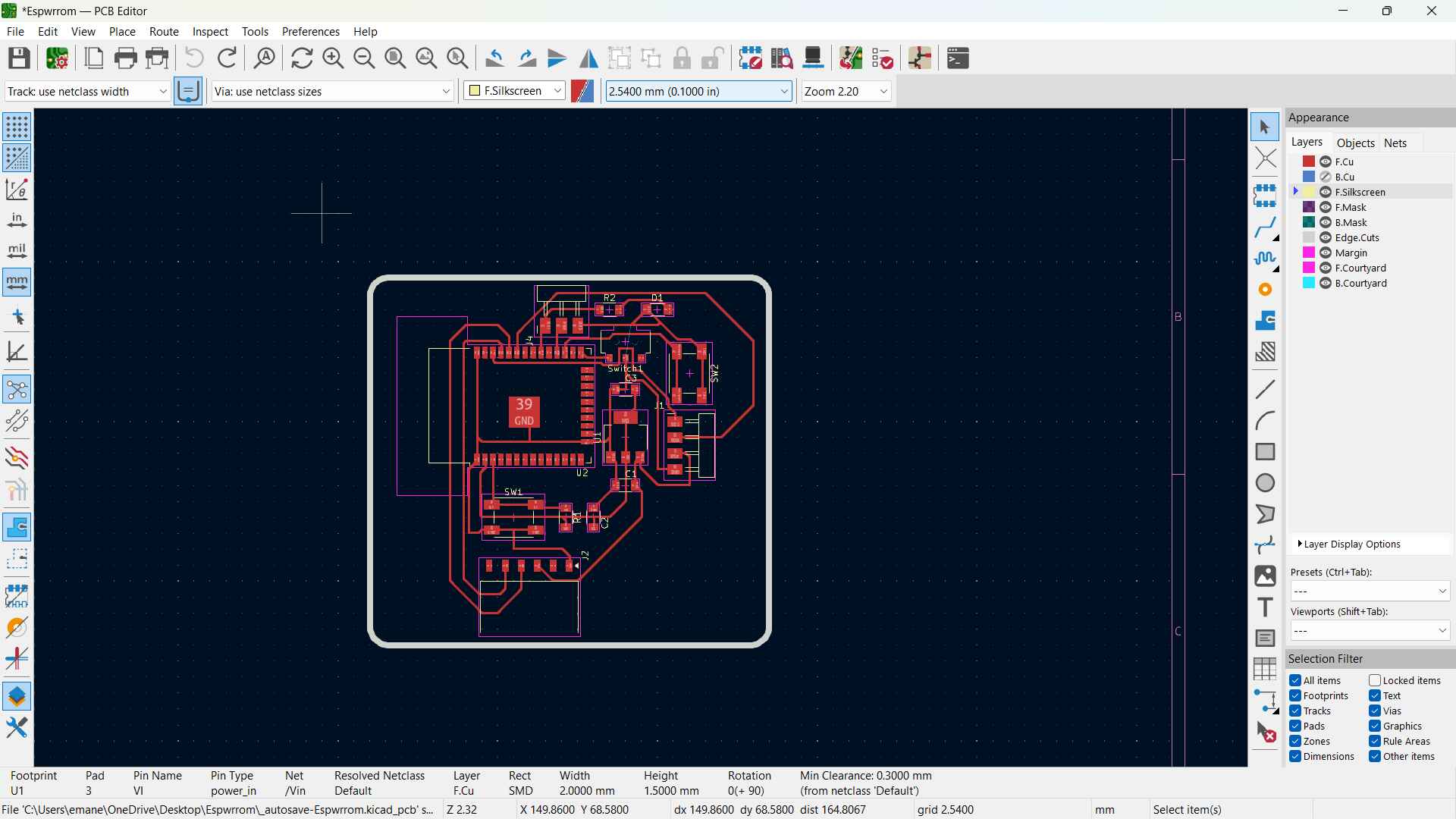
PCB Design in KiCad
Importing the Fab Library
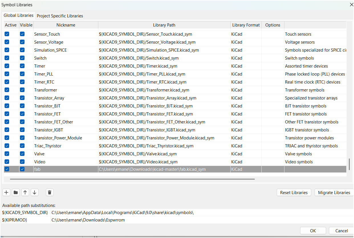
I started by downloading the fab library from the Fabacademy Gitlab as a ZIP File then imported it to my KiCad.I followed the instructions as written in the repo.
Schematic
-
Step 1
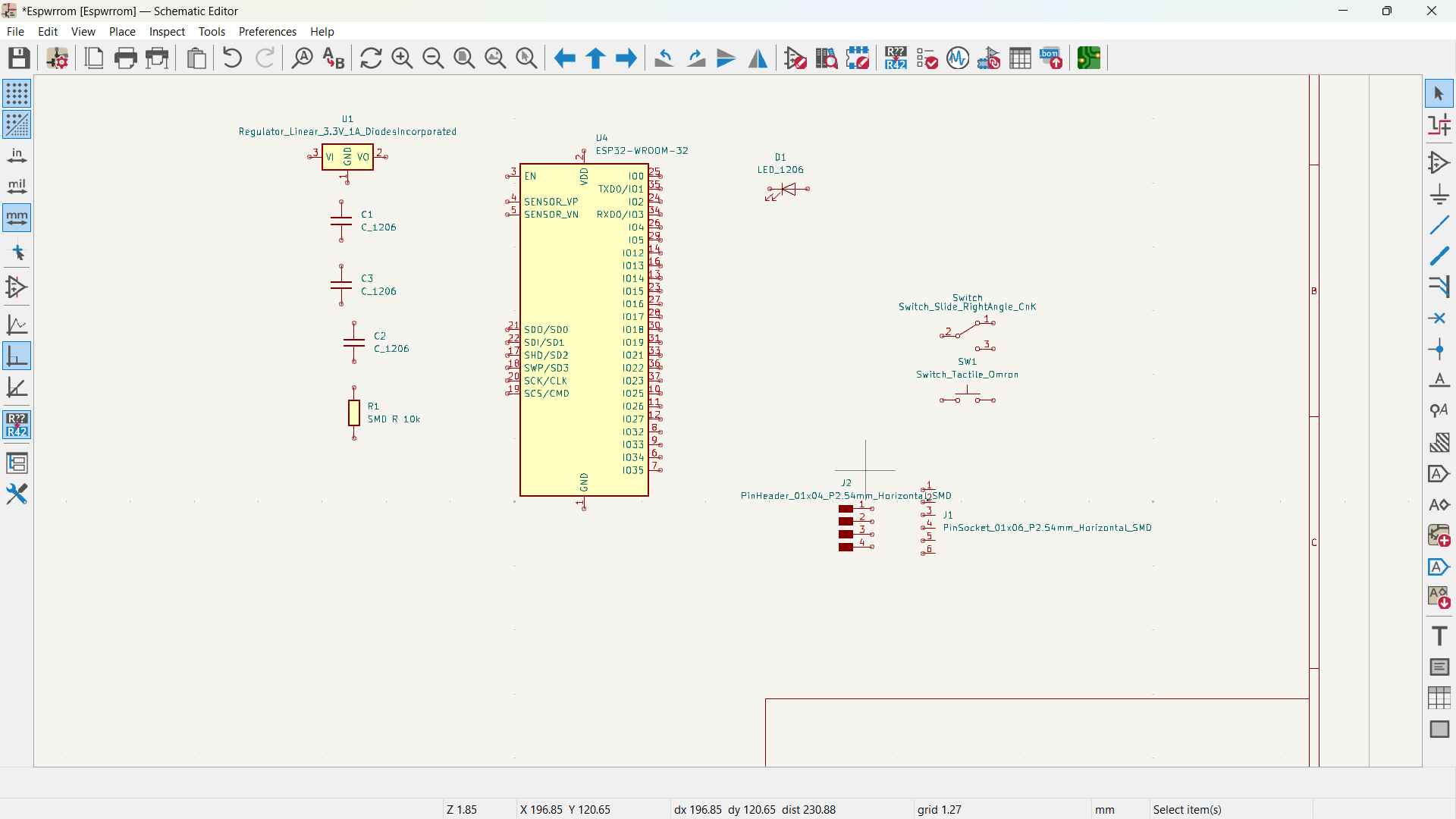
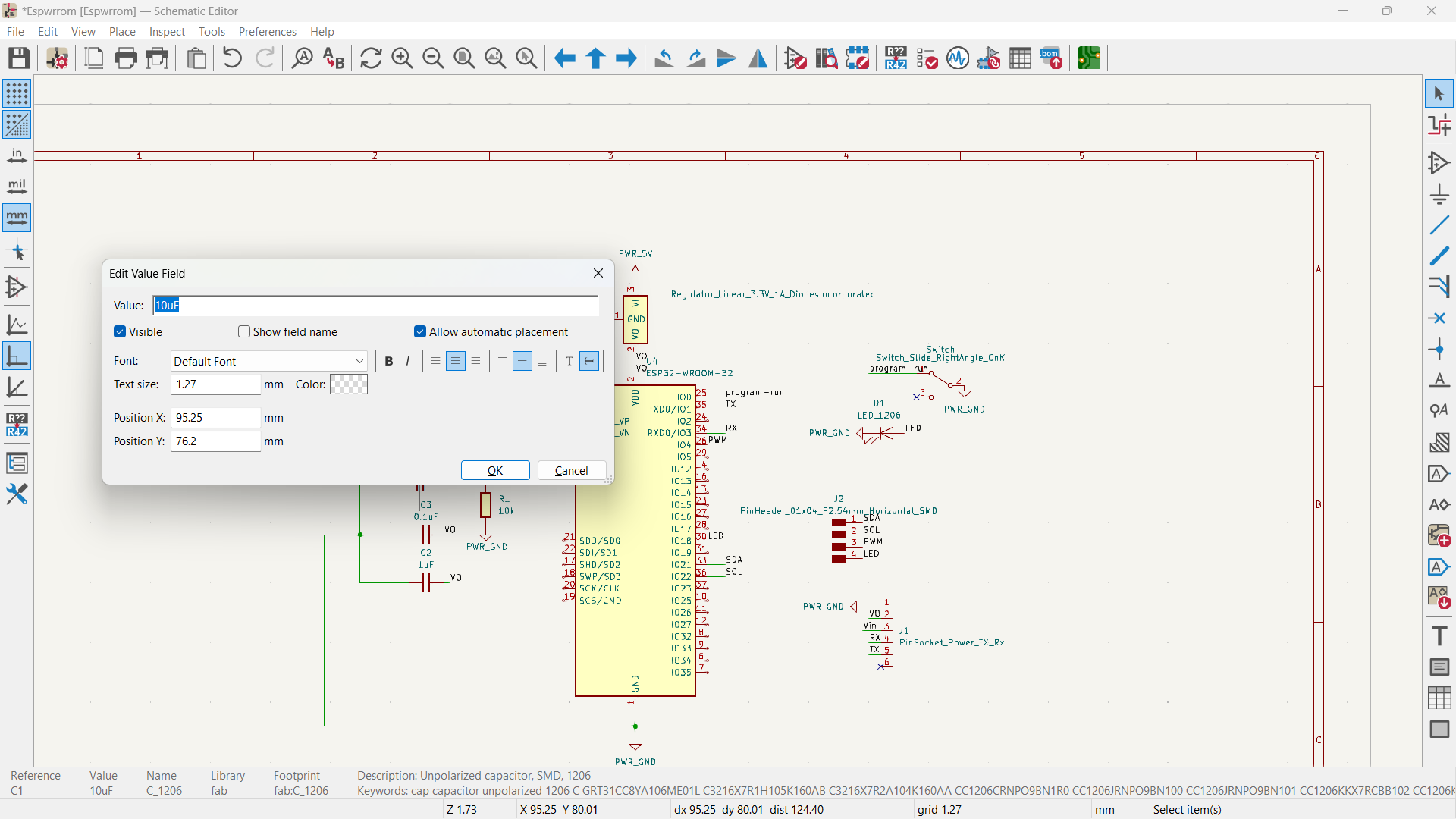
Created a project and Add all the components in the schematic note: I forgot the resistor for the LED and the button in this step but I added them afterwards.
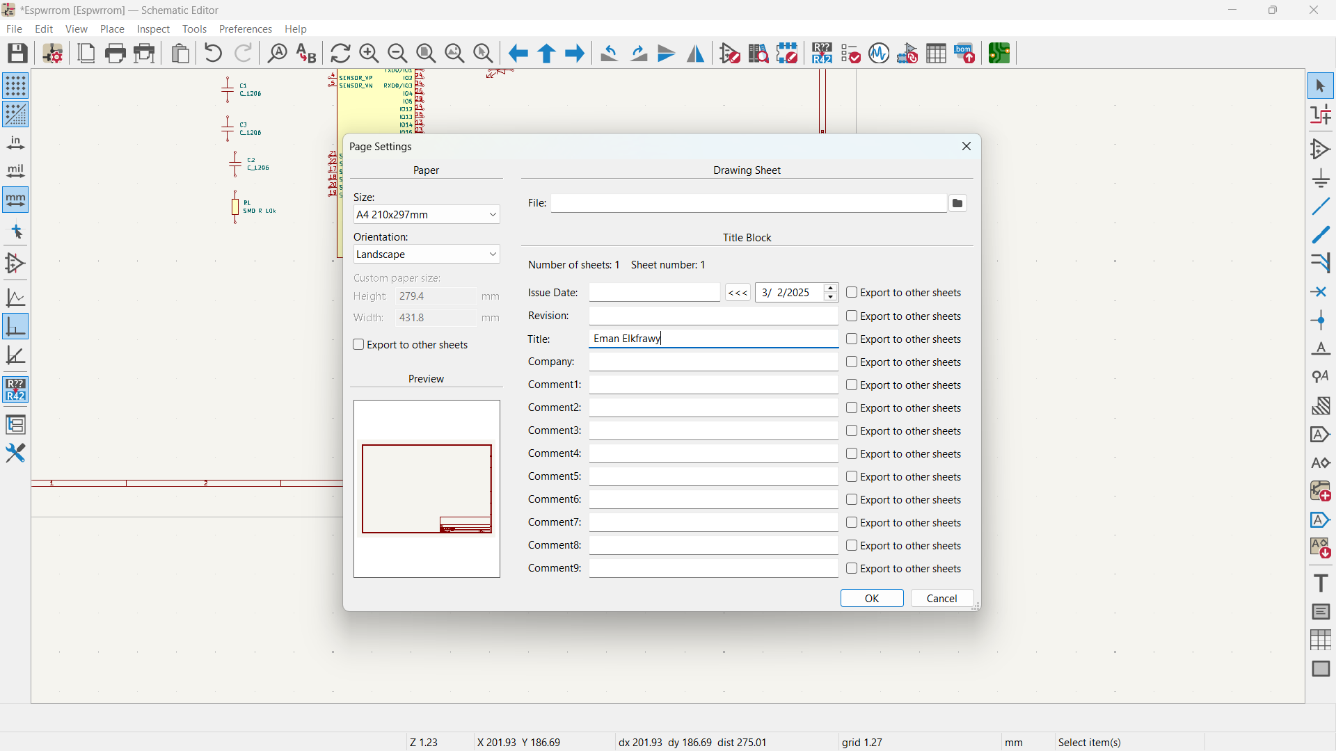
Gave a title
-
Step 2
Ground all the Components and start annotating.
-
Step 3
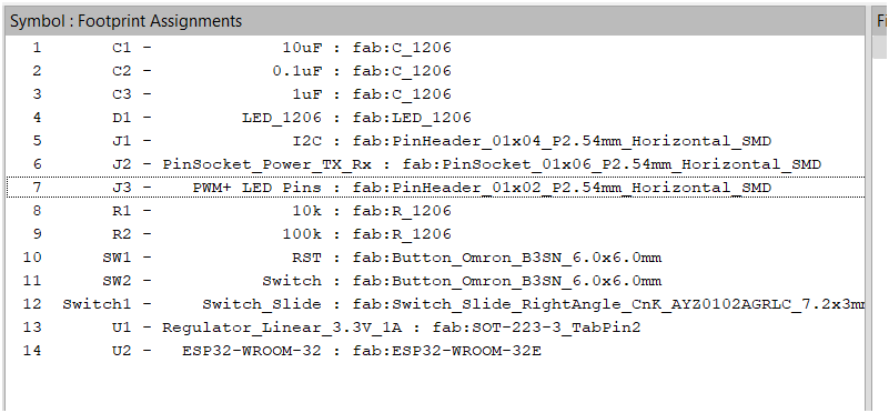
Assigning footprints
Final Edits
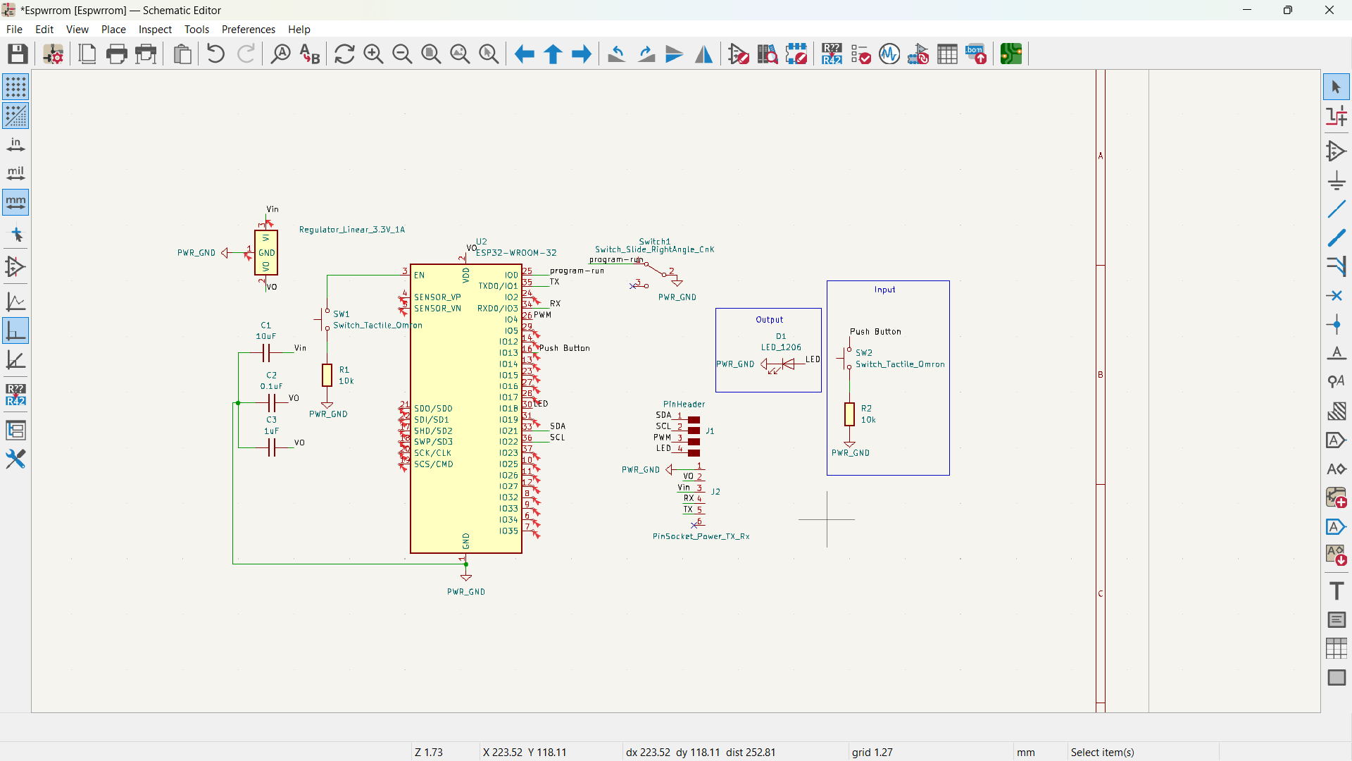
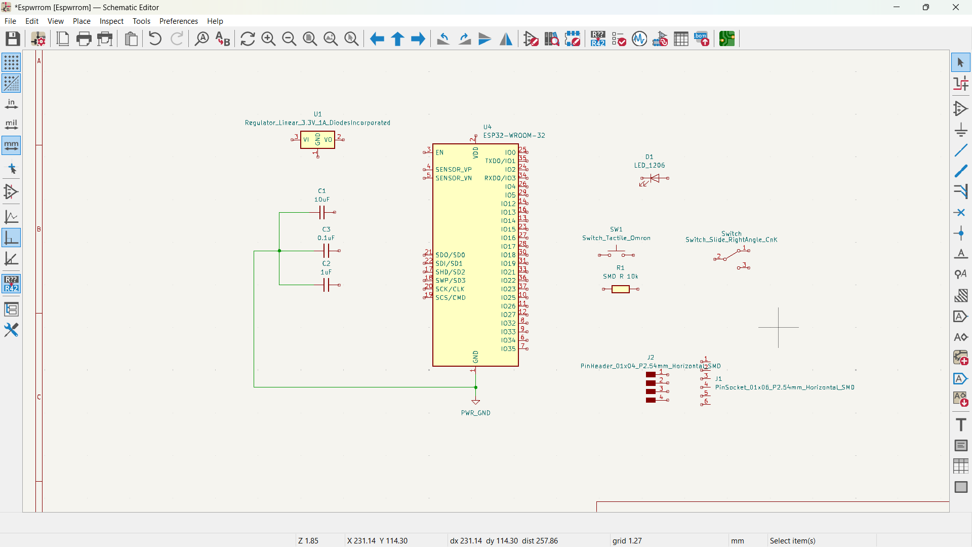
Final Schematic
.png)
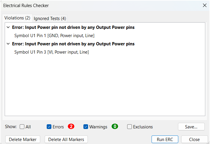
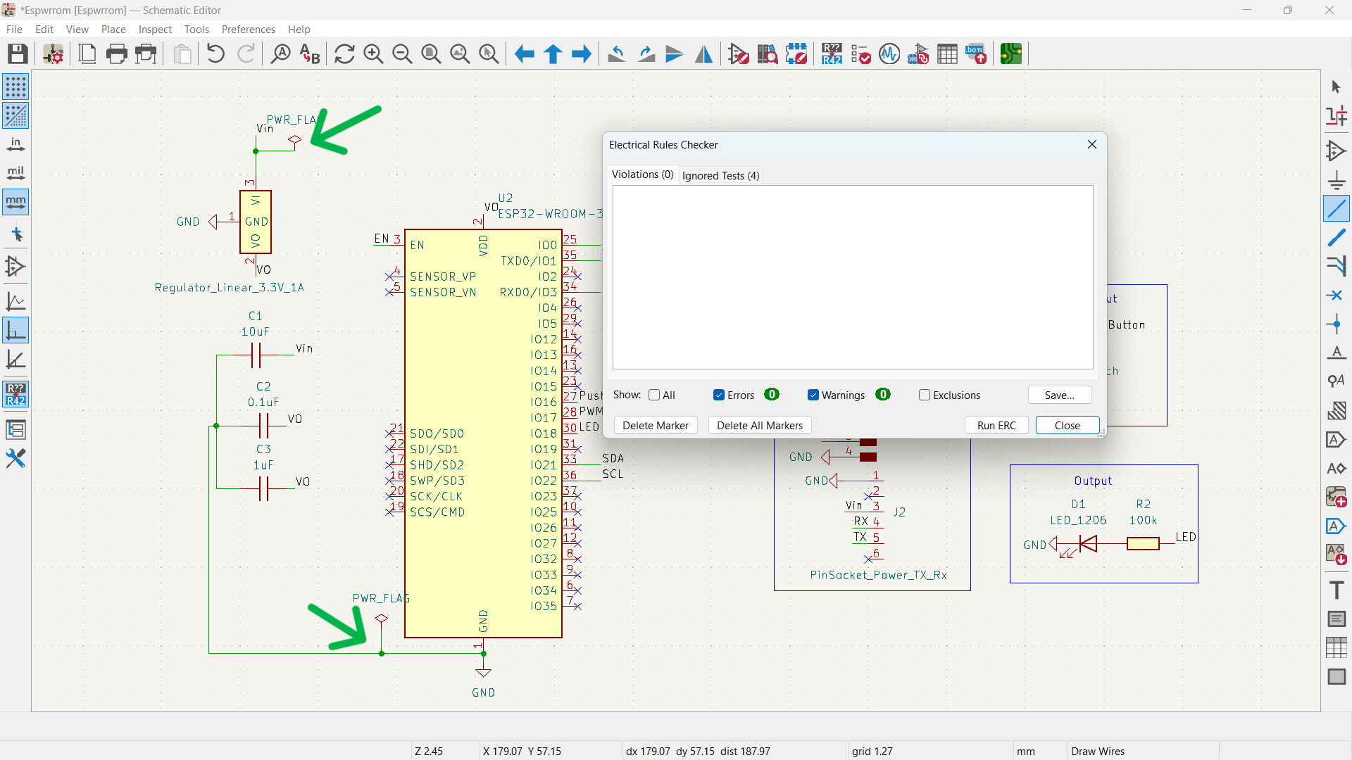
ERC
The ERC kept desplaying this message regarding the Connection to Vin. I inserted a power flag and it was resolved.
PCB Editor
-
From Schematic to PCB Editor
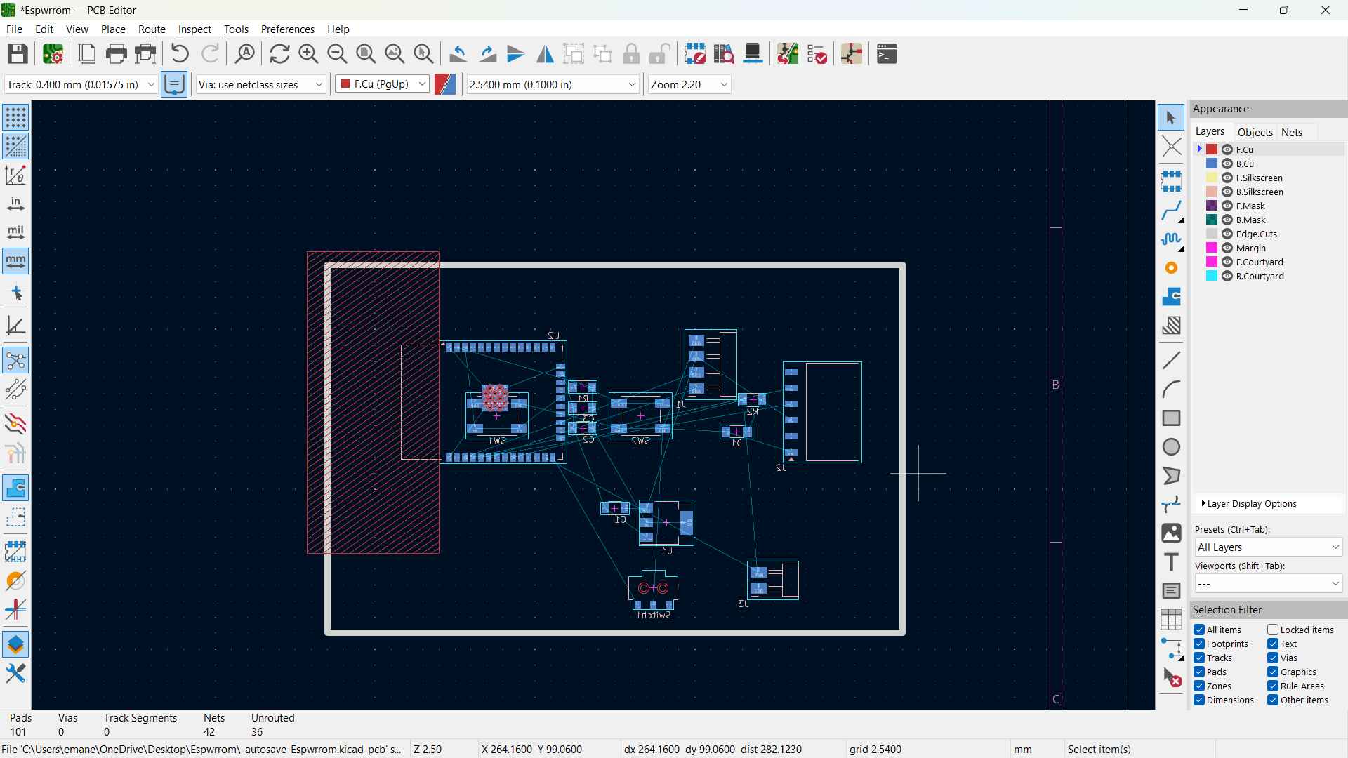
Once we're done with our schematic we click on the update pcb button
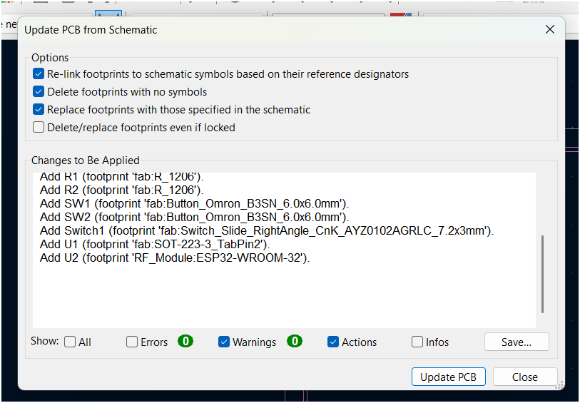
Once changed I found some component in the Cu:F and some in the Cu:B. To combine them in one layer I used Ctrl + F
-
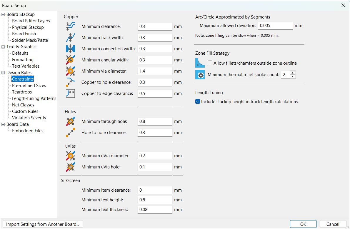
Routing and Design Rules
To make sure our pcb can be manufactured using our CNC milling machine. They depend mostly on your endmill diameter and the tolerance of the machine itself. I updated the Design Rules from Properties accordingly. At first I used a clearance of 0.4 but that resulted in some issues in the Design Rules Check because of the esp32 pads need a 0.3 endmill.
Then the tedious Routing quest began!
I created the outline using a rectangle and the fillet tool
-
DRC + 3D View
DRC results show that the slide switch's pad doesn't equal to the clearance, It has to with the switch's footprint.
3D View
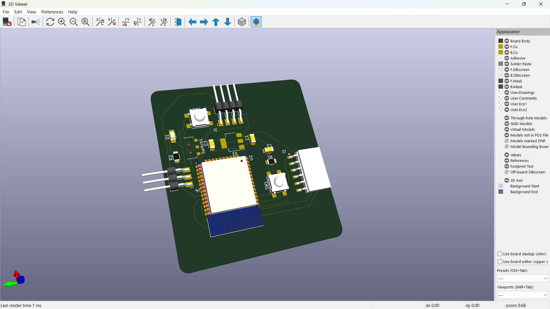
Final PCB